What Is a Monolithic Integrated Circuit?
A Monolithic Integrated Circuit places multiple electronic functions on one semiconductor substrate, usually silicon. Instead of wiring separate transistors, resistors, and capacitors across a circuit board, engineers form them together inside a tiny chip. This approach reduces electrical distance, manufacturing complexity, and physical size. It also improves consistency when millions of components must operate at high speed.
Semiconductor pioneer Gordon Moore gave this field a useful technical perspective: “The number of transistors incorporated in a chip will approximately double every 24 months.” His observation helps explain why Monolithic Integrated technology has progressed from simple logic devices to powerful processors, memory chips, sensors, and communication systems. The statement was not a permanent law, however. Manufacturing costs, heat, leakage current, and atomic-scale limits now challenge that pace.
Look closely at a modern chip package. The black rectangle may fit beneath a fingernail, yet its silicon core can contain intricate layers of metal interconnects. Each layer must align accurately during fabrication. A small defect can reduce yield or disable a complete device. This makes process control, circuit design, testing, and materials research equally important.
The term can sound simpler than the engineering really is. “Monolithic” does not mean every function is equally easy to integrate. Power components, optical elements, and high-performance analog circuits may require different structures or materials. A careful explanation should therefore separate the concept from marketing claims. Understanding these trade-offs reveals why Monolithic Integrated Circuits remain central to modern electronics, while also showing where their advantages begin to weaken.
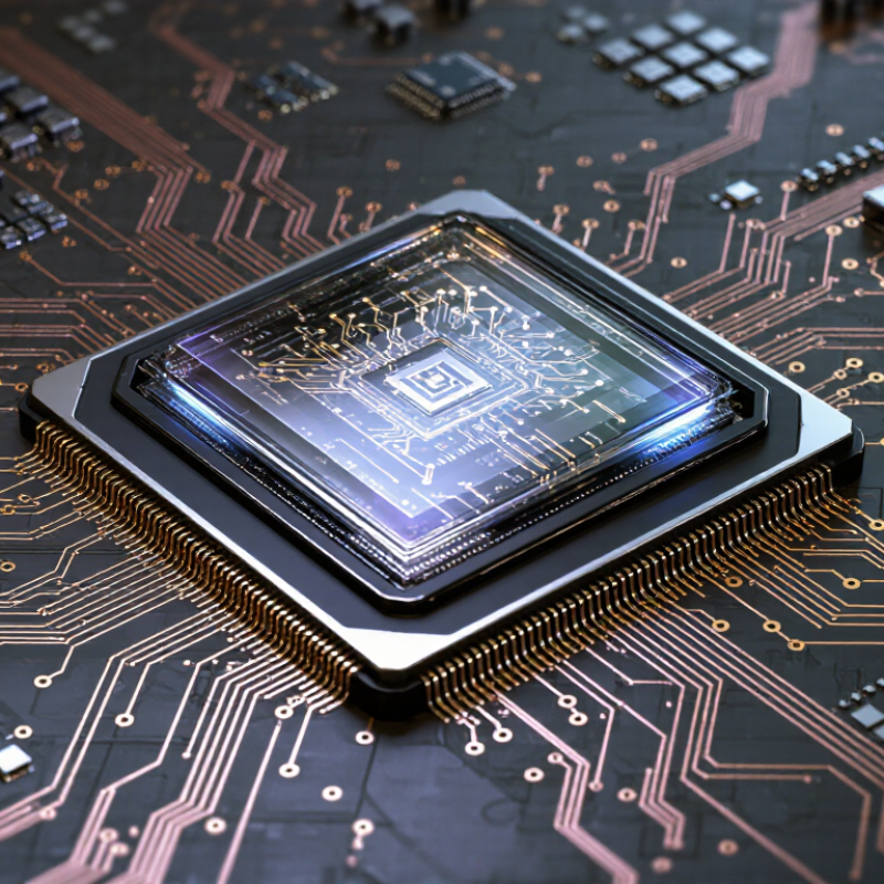
Definition and Structure: One Silicon Die Can Integrate Billions of Transistors
A monolithic integrated circuit places transistors, capacitors, resistors, and wiring on one silicon die. Manufacturers form these structures through repeated deposition, lithography, etching, and doping steps. The result resembles a tiny city, with metal layers acting like roads above active devices.
One silicon die can now integrate billions of transistors. The 2023 International Roadmap for Devices and Systems identifies continued scaling, advanced transistor structures, and backside power delivery as major development paths. These features help engineers fit more computing logic into limited area. They also create difficult problems. Power density rises, heat becomes harder to remove, and microscopic defects can reduce yield.
The definition sounds simple. It is not.
A monolithic design usually improves signal speed because nearby devices share short interconnects. It can also reduce package connections and system size. However, larger dies are not automatically better. A single defect may affect a greater area, increasing manufacturing risk. The Semiconductor Industry Association reported global semiconductor sales of 526.8 billion dollars in 2023, reflecting the enormous scale behind these manufacturing demands. Yet sales data does not measure technical quality by itself. Engineers must still balance transistor density, power consumption, thermal behavior, reliability, and production yield. That balance remains imperfect, especially as wiring delays and heat challenge further scaling.
What Is a Monolithic Integrated Circuit?
A monolithic integrated circuit places transistors, interconnections, and other circuit elements on a single silicon die. The chart shows representative, rounded transistor-count milestones demonstrating how one die evolved from thousands of transistors to tens of billions.
Values are approximate published industry milestones, rounded for comparison. The logarithmic scale makes changes across several orders of magnitude easier to read.
Fabrication Workflow: CMOS ICs Move from 300 mm Wafers to 3 nm Nodes
What Is a Monolithic Integrated Circuit?
A monolithic integrated circuit places transistors, wiring, and passive elements on one silicon die. Its fabrication begins with a polished 300 mm wafer, roughly the width of a dinner plate. Engineers clean, oxidize, and coat its surface before repeated lithography steps. Each pattern defines gates, contacts, or metal interconnects. Deposition, plasma etching, ion implantation, and chemical-mechanical polishing then shape microscopic layers. Tiny defects matter.
At a 3 nm node, the label does not mean every feature measures three nanometers. It describes a process generation with tighter density, power, and performance targets. The 2024 International Roadmap for Devices and Systems links advanced nodes with increasingly complex patterning and process control.
Meanwhile, SEMI’s World Fab Forecast projected global 300 mm capacity above 9 million wafers per month during 2025. That scale explains the workflow’s discipline: one particle can damage many dies. Metrology checks line edges, film thickness, overlay, and electrical behavior after critical steps. Wafers may pass through hundreds of operations before dicing and packaging.
The cleanroom looks calm, but the process is not simple. A neat diagram can hide rework, yield losses, and difficult tradeoffs between speed, leakage, and manufacturing cost. Even the 3 nm name can mislead readers without a physical-dimension explanation.
Scale Benchmark: Apple’s 3 nm M3 Chip Integrates 25 Billion Transistors
What Is a Monolithic Integrated Circuit?
A monolithic integrated circuit places transistors, wiring, and functional blocks on one silicon die. This structure differs from multi-chip designs, where separate dies communicate through a package. The advantage is shorter electrical paths. That can reduce signal delay, energy loss, and packaging complexity. It also creates difficult manufacturing constraints.
A useful scale benchmark is a 3-nanometer processor integrating about 25 billion transistors. That figure comes from the processor specification widely reported for this class of chip. It shows how far monolithic integration has advanced. However, transistor counts can mislead. More transistors do not automatically deliver better real-world performance. Architecture, memory access, software, and thermal limits still matter.
Small geometry, large consequences.
The Semiconductor Industry Association reported that global semiconductor sales reached approximately 526.9 billion dollars in 2023. Meanwhile, the International Roadmap for Devices and Systems identifies power density, interconnect delay, and manufacturing variability as continuing industry challenges. These reports support a cautious interpretation: scaling remains valuable, but it is no longer a simple size contest. Modern 3-nanometer labels also describe a manufacturing generation, not every physical feature measuring exactly three nanometers. I have found this distinction important when comparing technical claims. A dense die may look like a city viewed from above, yet one congested road can slow the entire system. That imperfect analogy still exposes the central engineering problem: integration increases capability, while coordination determines usefulness.
What Is a Monolithic Integrated Circuit? — Scale Benchmark: A 3 nm Chip Integrates 25 Billion Transistors
Key characteristics and scale indicators of monolithic integrated circuits | Dimension | Measured or Defined Value | Technical Meaning |
| Integration type | Monolithic | Transistors, resistive elements, capacitive structures, and interconnections are fabricated on the same semiconductor die. |
| Reference process node | 3 nm class | A modern semiconductor process-generation label; it should not be interpreted as the exact physical length of every transistor feature. |
| Integrated transistor count | Approximately 25 billion | A single advanced processor die can contain roughly 25,000,000,000 individually fabricated transistor devices. |
| Transistor-count scale | 25 billion : 1 | The ratio indicates that the die contains about 25 billion switching devices rather than a single discrete component. |
| Unit conversion | 3 nm = 0.000003 mm | One nanometre equals one-millionth of a millimetre; the conversion describes the unit scale, not a universal chip dimension. |
| Electrical function | Switching and signal processing | Transistors act as controllable switches that implement logic, memory elements, amplification, and data-processing functions. |
| Primary substrate | Silicon wafer | The circuit is formed in and above a silicon substrate using repeated deposition, patterning, etching, doping, and metallization steps. |
| Interconnection method | On-die metal layers | Multiple patterned metal layers connect devices across the die and route power, clock, control, and data signals. |
| Main advantage | High density and short internal connections | Integrating components on one die can reduce package-level wiring, improve signal efficiency, and support compact system designs. |
| Typical trade-off | Manufacturing complexity | A defect affecting one die can reduce yield, while advanced patterning and multilayer fabrication require highly precise manufacturing processes. |
Note: The 25-billion-transistor figure is presented as a reference scale for an advanced 3 nm-class processor. Process-node names are industry labels and do not represent one uniform physical measurement across the entire die.
Main Categories: Analog, Digital, Mixed-Signal, and RF Monolithic ICs
What Is a Monolithic Integrated Circuit?
A monolithic integrated circuit places transistors, resistors, capacitors, and interconnections on one semiconductor die. The die may fit inside a small black package. This construction shortens signal paths, improves repeatability, and supports high-volume manufacturing. However, heat, noise, and process limits still shape its performance.
Analog monolithic ICs process continuously changing voltages or currents. They appear in sensor interfaces, voltage regulators, amplifiers, and timing circuits. Designers often evaluate offset voltage, noise density, bandwidth, and temperature drift. Digital monolithic ICs handle defined logic states, usually represented by binary values. They power processors, memory devices, controllers, and communication logic. Switching speed matters, but leakage, power consumption, and electromagnetic noise matter too. A fast circuit is not automatically efficient.
Mixed-signal monolithic ICs combine analog functions with digital processing. A data converter may sample a microphone signal, quantize it, and send digital words to a controller. Layout becomes demanding because digital switching can disturb sensitive analog nodes. RF monolithic ICs operate with high-frequency signals for wireless links, radar, and positioning equipment. They require careful impedance control, low-noise design, and stable frequency generation. In practice, category boundaries can blur. An RF receiver may include analog filtering and digital calibration. Engineers should verify specifications under real temperature, supply, and load conditions. Laboratory results can look cleaner than field behavior. That gap deserves attention.